
Introduction :
We all know about semiconductors, right? What do intrinsic semiconductors and extrinsic semiconductors mean? Furthermore, what is the difference between intrinsic and extrinsic semiconductors? In this post, we are going to figure out the answer to all these questions through a detailed understanding of intrinsic and extrinsic semiconductors.
Semiconductors :
Semiconductors are an unusual type of material; however, their electrical conductivity is lower than that of conductors and higher than that of insulators. Moreover, semiconductors are classified into two types: intrinsic semiconductors and extrinsic semiconductors. This classification is based on the type and number of contaminants added to improve their electrical and optical properties.
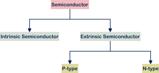
Classification of semiconductors :
The following diagram provides the classification of semiconductors.
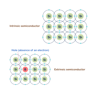
Intrinsic semiconductors :
The pure form of semiconductors is called intrinsic semiconductors. In intrinsic semiconductors, no impurities are added. As a result, intrinsic semiconductors do not have impurities inside them, and this absence of impurities does not improve their electrical and optical properties. So, it doesn’t have more practical applications like extrinsic semiconductors in electronics.
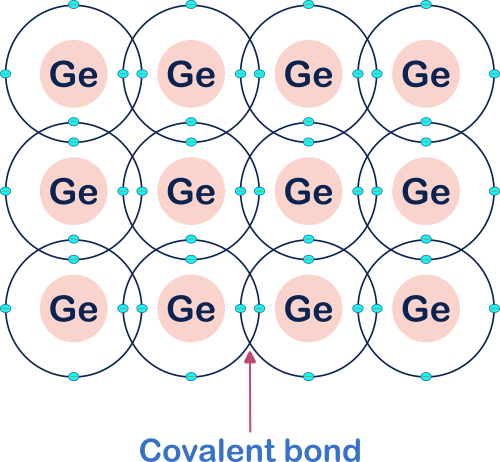
Crystal structure of Intrinsic semiconductors :
Here, I present the crystalline structure of the pure Silicon (Si) and pure Germanium (Ge) semiconductors. Let me consider only the valence shell of the Silicon (Si) and Germanium (Ge) atoms.
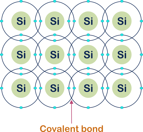
In the above crystal diagrams of intrinsic semiconductors, as depicted, a covalent bond connects all the valence electrons of the neighboring intrinsic semiconductor atoms. To become free electrons, the valence electrons must expend a significant amount of energy to break this covalent bond.
Free electrons and holes (considering holes as the absence of electrons) play a crucial role in enabling electric current flow within the semiconductor material. However, in the case of intrinsic semiconductors, there are not enough free electrons and holes at room temperature. Consequently, their electrical conductivity is not particularly high.
Extrinsic semiconductors :
By now, we know that the intrinsic semiconductor’s electrical conductivity is not that good. Then, how can we increase the electrical conductivity of the intrinsic semiconductor (or) semiconductor in general? Yes, what you think is correct, by adding some impurities to the intrinsic semiconductors.
When we add some impurities into the intrinsic semiconductors, then that is known to be Extrinsic semiconductors. By doing this, we can increase the electrical conductivity of the semiconductors.
Crystal structure of Extrinsic semiconductors :
Here, I am providing the crystalline structure of the N-type extrinsic semiconductor. Specifically, I am considering Germanium (Ge) as the semiconductor atom and Phosphorus (P) as the pentavalent impurity atom. In this context, I am focusing solely on the valence shell of the Germanium (Ge) and Phosphorus (P) atoms.
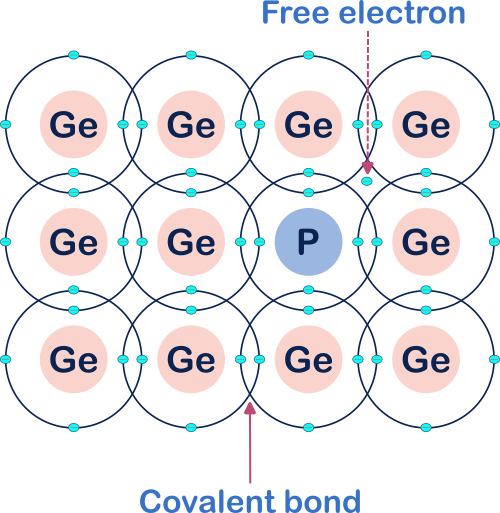
In the above crystal diagram of Extrinsic semiconductors, you see even at room temperature the semiconductors have enough free electrons for electrical conduction due to the added impurity. This phenomenon makes Extrinsic semiconductors more suitable for practical electronics applications.
Extrinsic semiconductors are further classified into two types. Those are,
- P-type semiconductors
- N-type semiconductors
1. P-type semiconductors :
When we dope the intrinsic semiconductor with the trivalent impurity atom, the resultant extrinsic semiconductor will be a P-type semiconductor.
The reason for the name, P-type semiconductor
We are getting P – Type semiconductors by doping the intrinsic semiconductor with the tri-valent impurities. Here Tri means 3. In trivalent impurities, the valence shell has 3 electrons. When the semiconductor atom forms a covalent bond with the nearby trivalent impurity atom, there will be an absence of one electron in the covalent bond, so the absence of one electron is mentioned as a hole (positive charge). P means positive. Here, in a P-type semiconductor, we are getting one extra hole for including one trivalent impurity atom, that’s why it is called a P-type semiconductor.
Crystal structure of P-type semiconductor :
Here, I am presenting the crystalline structure of the P-type semiconductor. Specifically, I am using silicon (Si) as the semiconductor atom and Boron (B) as the trivalent impurity atom. In this context, I am focusing exclusively on the valence shell of the Silicon (Si) and Boron (B) atoms.
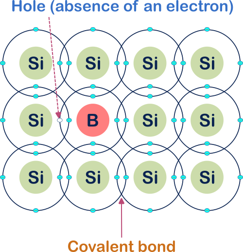
Here, we dope the Silicon (Si) atom with a trivalent impurity atom, Boron (B), to create a P-type semiconductor. Boron has 3 valence electrons and Silicon has 4 valence electrons. So 3 out of 4 valence electrons in the Silicon (Si) atom, form covalent bonds with the boron atom’s valence electrons. The remaining valence electron of Silicon (Si) doesn’t have a pair to complete the covalent bond with the Boron impurity atom. So, the absence of electrons in that specific covalent bond is considered a hole, which is a positively charged carrier.
Due to this doping, we generated free charge carriers (holes) inside the P-type semiconductor. This will improve the electrical conductivity of the extrinsic semiconductor slightly.
In P-type semiconductors,
What is meant by a trivalent impurity atom?
If the number of electrons in the atom’s valence shell is 3, then that kind of atom is called as trivalent atom. Here, “tri” means Three (3).
Examples for trivalent impurity atom :
- Boron (B)
- Aluminium (Al)
- Gallium (Ga) etc.,
2. N-type semiconductors :
When we dope the intrinsic semiconductor with the pentavalent impurity atom, the resultant extrinsic semiconductor will be an N-type semiconductor.
The reason for the name, N-type semiconductor
We are getting N-type semiconductors by doping the intrinsic semiconductor with the pentavalent impurities. Here Penta means 5. In pentavalent impurities atom, the valence shell has 5 electrons. When the semiconductor atom having 4 valence electrons (like Si, Ge, etc.,) forms a covalent bond with the nearby pentavalent impurity atom, there will be one extra electron available in the valence shell of the pentavalent impurity atom. So this existence of one electron is mentioned as a negative charge. N means negative. Here, in a N-type semiconductor, we are getting one extra electron for adding one impurity atom, that’s why it is called a N-type semiconductor.
Crystal structure of N-type semiconductor :
Here, I am presenting the crystalline structure of the N-type semiconductor. In this representation, I am using silicon (Si) as the semiconductor atom and Phosphorus (P) as the pentavalent impurity atom. For clarity, I am specifically considering only the valence shell of the Silicon (Si) and Phosphorus (P) atoms.
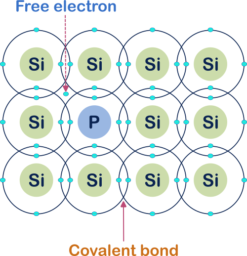
Here, we dope the Silicon (Si) atom with a pentavalent impurity atom, Phosphorus (P), to form an N-type semiconductor. Phosphorus has a five valence electron and Silicon has a four valence electron. The 4 valence electrons in silicon (Si) form covalent bonds with the Phosphorus (P) atom’s 4 valence electrons. The remaining valence electron of Phosphorus (P) doesn’t have a pair to complete the covalent bond with the Silicon (Si) atom. So, in this process, the Phosphorus (P) atom releases one extra electron, allowing it to move freely within the material. In simpler terms, it generates one free electron.
Due to this doping, we generated free charge carriers (electrons) inside the N-type semiconductor. This will improve the electrical conductivity of the extrinsic semiconductor slightly.
In N-type semiconductors,

What is meant by a pentavalent impurity atom?
If the number of electrons in the atom’s valence shell is 5, then that kind of atom is called a pentavalent atom. Here Penta means 5.
Examples for pentavalent impurity atom :
- Phosphorus (P)
- Arsenic (As)
- Antimony (Sb) etc.,
What is doping?
Doping is the process of adding impurities to the pure form of the semiconductor to convert it into an extrinsic semiconductor.
Doping is the process of intentionally introducing specific impurity atoms or molecules into a semiconductor material to modify its electrical properties. Typically, people do this to increase the number of charge carriers (electrons or holes) in the material or to alter its conductivity and other semiconductor characteristics. Doping is a crucial technique in semiconductor device manufacturing, as it allows for the precise control of a semiconductor’s electrical behaviour, making it suitable for various electronic applications.
The following table shows the multiple levels of doping,
| Doping level | impurity atom : pure atom | Notation |
|---|---|---|
| Moderate doped | 1 : 106 to 108 | P , N |
| Lightly doped | 1 : 1011 | P–, N– |
| Heavily doped | 1 : 103 | P+, N+ |
Summary :
- Intrinsic semiconductor is the pure form of semiconductor.
- Adding impurities to the intrinsic semiconductor results in an extrinsic semiconductor.
- P-type (trivalent impurity added)
- N-type (pentavalent impurity added)
- Doping is the process of adding impurities to the semiconductor.
22 Responses
It is a pleasure to read this weblog, thanks to its up-to-date information and interesting posts.
Informative articles, excellent work site admin! Cheers to creating useful content on the web!
I’m really enjoying the design and layout of your site.
It’s a very easy on the eyes which makes it much more enjoyable
for me to come here and visit more often. Did you hire out
a designer to create your theme? Exceptional work!
I love it when folks come together and share ideas.
Great site, stick with it!
I absolutely love your site.. Pleasant colors & theme.
Did you build this web site yourself? Please reply back as
I’m hoping to create my own personal blog and would like to learn where you
got this from or what the theme is named.
Many thanks!
Hey! This post couldn’t be written any better! Reading this post reminds me of my previous room
mate! He always kept talking about this. I will forward this page to
him. Pretty sure he will have a good read. Thank you for sharing!
Good day! I just wish to give you a big thumbs up for your great information you’ve got right here on this post.
I’ll be returning to your web site for more soon.
Greetings from Ohio! I’m bored to death at work so I decided to browse your site on my
iphone during lunch break. I really like the information you provide here and can’t wait to take a look when I
get home. I’m shocked at how fast your blog loaded on my phone ..
I’m not even using WIFI, just 3G .. Anyhow, great blog!
Hi! Would you mind if I share your blog with my facebook group?
There’s a lot of folks that I think would really appreciate your content.
Please let me know. Thank you
Yes, You can!!!
Have you ever thought about writing an ebook or guest authoring on other blogs?
I have a blog based on the same information you discuss and would really like
to have you share some stories/information. I know my visitors would appreciate your work.
If you are even remotely interested, feel free to shoot me an e-mail.
Nice response in return of this difficulty with genuine arguments and describing the whole thing about that.
Wow, this post has given me useful info and answered some of my questions. I hope to give something back and aid others like you helped me.
partai togel partai togel
partai togel
It’s in fact very complex in this busy life to listen news
on Television, therefore I simply use internet for that purpose, and get the most recent news.
Hello, i feel that i saw you visited my weblog thus i came
to return the choose?.I am attempting to to find issues to enhance my site!I assume its adequate to make use of some
of your concepts!!
With havin so much content do you ever run into any problems of
plagorism or copyright violation? My blog has a lot of completely unique content I’ve either authored
myself or outsourced but it seems a lot of it is popping it up all over the internet without my agreement.
Do you know any ways to help reduce content from being stolen? I’d certainly
appreciate it.
I think that what you said made a great deal of sense.
However, what about this? what if you composed a catchier title?
I am not saying your content isn’t good., however what if you
added a post title that makes people desire more?
I mean What are Intrinsic semiconductors
and Extrinsic semiconductors? – V Edifys is a little boring.
You might look at Yahoo’s home page and watch how they create
article titles to grab viewers interested. You might add a related video or a picture or two to
get people excited about what you’ve written. In my opinion, it would bring your
posts a little bit more interesting.
Great post.
Thank you for the auspicious writeup. It in fact was a amusement
account it. Look advanced to far added agreeable from you!
However, how could we communicate?
just contact me via a contact form in the menu
Wonderful beat ! I would like to apprentice while you amend your website, how could i
subscribe for a blog site? The account helped me a applicable deal.
I had been tiny bit acquainted of this your broadcast offered shiny
clear idea
I am really impressed together with your writing abilities and also with the layout to your blog. Is this a paid theme or did you customize it your self? Anyway keep up the excellent high quality writing, it is uncommon to see a great weblog like this one today!