

Introduction :
We all study about the energy bands of materials in our physics classes. But what does this entail, and why is it crucial knowledge? Understanding energy bands is essential as it intricately defines the electrical behaviour of materials, particularly semiconductors. In this discussion, we’ll explore the significance of energy bands, their implications, their classification and how they provide insights into the electrical properties of various materials, especially semiconductors.
What are Energy bands in general?
In simple terms, “bands” refer to groups of something. So, when we talk about “Energy bands,” we’re referring to groups that consist of multiple distinct energy levels combined.
Understanding of energy bands through atomic structure :
Let’s consider the Niels Bohr’s atomic model of Silicon (Si) atom.
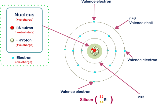
Let’s examine the image. The atomic model designates the outermost shell as the valence shell, and the electrons in this shell are referred to as valence electrons. Each electron in an atom possesses a unique energy level. Depending on these energy levels, the electrons orbit around the nucleus in specific orbits. Consequently, each shell in the atom encompasses distinct energy levels. The group of this distinct energy levels is known to be energy bands in general. e.g. valence band and conduction band.
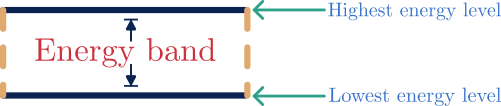
Generally, we are representing the energy bands with the two horizontal lines. The lower line represents the lower level of energy in that particular energy band and the upper line represents the higher level of energy in that particular energy band. This is given in the below picture,
There are two major energy bands that we need to understand about any materials in general, semiconductors in particular. Those are,
- Valence band
- Conduction band
Valance band :
Now, we know about the valence shell and valence electrons. Then what is meant by a valence band? Each electron in the valence shell does have distinct levels of energy. Why is that the case? Every material is made up of a large number of atoms. If a valence electron of a particular atom, has attracted by the nucleus of the nearby atom then it will lose some of its energy in that process. Valence electrons are in the outermost shell of an atom. There may be friction between the valence electrons of two nearby atoms, in this process also they may lose some energy.
Due to these reasons, the valence electrons of any atom may have different energy levels from one another. So, these different energy level of valence electrons forms a group of energy level that is known to be valence band.
Conduction band :
By this time, we all know about the conduction electrons. If you don’t know, here is a simple explanation. The valence electrons always tend to free themself from the attractive force of their atomic nucleus. For this, they require some energy, obtained from temperature, light, etc. When the atoms are at room temperature, the valence electrons gain the necessary energy to break free from the attractive force of the nucleus. As a result, they behave like free electrons.
What is the relationship between free electrons and the conduction? Electrical conduction is only possible when we have sufficient free electrons in the material at room temperature. So, the free electrons are also called conduction electrons.
The free electrons roam freely inside the material. During this process, they may collide with the atoms and other free electrons that are in their path. So, in this process, the conduction electrons may lose some of their energy.
Because of this reason, the conduction (or) free electrons may have different energy levels from one another. So, these different energy level of conduction electrons forms a group of energy level that is known to be a conduction band.
Representation of conduction band and valence band :
By now you may understand that the charge carriers in the conduction band have higher energy levels than the charge carriers in the valence band. Because the charge carriers in the valence band absorb some energy to move into the conduction band. Generally, we need to draw the valence band below the conduction band.
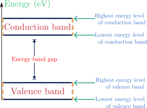
Now, you may have a doubt about the gap between the conduction and valence band. Why is this mentioned in the above diagram? This energy gap is known to be band gap energy (or) energy band gap. This band gap energy decides the material’s electrical conductivity properties. It shows, how much energy is required for the valence electron to go to the conduction band. If the longer the energy band gap is, the valence electron needs a larger amount of energy to go to the conduction band.
Energy band gap = Lower energy level of conduction band – Higher energy level of valence band
Energy bands of different materials :
Here, we are going to see the energy bands diagram of the conductor, semiconductor and insulator.
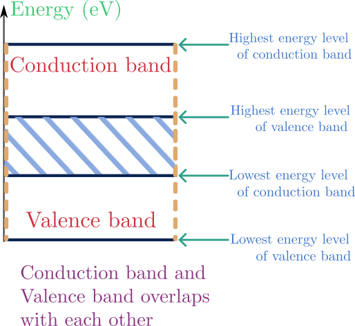
Conductors :
In conductors, the conduction band and the valence band overlap each other. What is meant by this at the atomic level? The valence electrons need only a small amount of energy to make themself as conduction electrons (or) free electrons. Due to the overlap of energy bands, the valence electrons in the conductors will get that needed energy to free themself as free electrons at room temperature as well. The energy band gap of conductors is zero. ( i.e. < 0 eV)
The below given diagram shows the energy band diagram of conductors.
Semiconductors :
In semiconductors, there is a separation of less than or equal to 5 eV between the conduction band and the valence band. What is meant by this at the atomic level? The valence electrons need less than or equal to 5 eV of energy (depending upon the material) to make themself as conduction electrons (or) free electrons. Due to the energy band gap, the valence electrons in the semiconductors will not get the needed energy to free themself as free electrons at room temperature. So, some other chemical (or) optical mechanisms are used in the semiconductors to create the required free electrons at room temperature.
The below given diagram shows the energy band diagram of semiconductors.
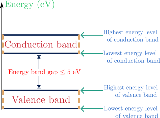
Energy band gap of some semiconductors :
Here, we have the energy band gap of Silicon (Si) and Germanium (Ge) at 300 K (room temperature).
- Energy band gap of Si = 1.1 eV
- Energy band gap of Ge = 0.7 eV
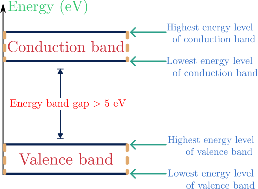
Insulators :
In insulators, there exists a separation of greater than 5 eV between the conduction band and the valence band. What is meant by this at the atomic level? The valence electrons need greater than 5 eV of energy (depending upon the material) to make themself as conduction electrons (or) free electrons. Due to the larger energy band gap, the valence electrons in the insulators will not get the needed energy to free themself as free electrons at room temperature. So, there are no free electrons in the insulators at room temperature, therefore it won’t conduct electricity at room temperature.
The below given diagram shows the energy band diagram of insulators.
Note :
Does this mean, insulators never conduct electricity? No, it can conduct electricity at a very high temperature. But, at that higher level of temperature the insulating material won’t survive, it will burn out. So, practically insulators won’t conduct electricity.
Summary :
- In general, we refer to the group of distinct energy levels as energy bands.
- There are two important energy bands that defines the electrical properties of the materials. Those are,
- Conduction band
- Valence band
- The energy band gap, also known as the band gap energy, designates the absolute difference between the lower energy level of the conduction band and the higher energy level of the valence band.
- Semiconductors energy band gap ≤ 5 eV.
- Insulators energy band gap > 5 eV.
- Conductors there will be no energy band gap because the conduction and valence bands overlap with each other.
16 Responses
Keep on working, great job!
Keep on working, gret job!
You’ve done an impressive work on your website in covering the topic.
Thank you for sharing this information!
Your style is really unique compared to other people I’ve read stuff from.
Thanks for posting when you’ve got the opportunity, Guess I’ll just bookmark this web site.
Your style is really unique compared to other people I’ve read stuff from.
Thanks for posting when you’ve got the opportunity, Guess
I’ll just bookmark this web site.
It’s remarkable in favor of me to have a website, which
is valuable designed for my know-how. thanks
admin
Very great post. I simply stumbled upon your weblog and
wished to say that I have really enjoyed surfing around your
weblog posts. In any case I will be subscribing for your rss feed and I’m hoping you write once more very soon!
Very great post. I simply stumbled upon your weblog and wished to say that I have really enjoyed
surfing around your weblog posts. In any case I will
be subscribing for your rss feed and I’m hoping you write once more very soon!
magnificent points altogether, you just won a new reader.
What may you recommend in regards to your post that you just made
some days in the past? Any positive?
magnificent points altogether, you just won a new reader.
What may you recommend in regards to your post
that you just made some days in the past? Any
positive?
Hello! I know this is kinda off topic nevertheless I’d figured I’d ask.
Would you be interested in trading links or maybe guest authoring a blog post or vice-versa?
My site covers a lot of the same subjects as yours and
I feel we could greatly benefit from each other. If you are interested feel
free to send me an email. I look forward to hearing from you!
Great blog by the way!
Hello! I know this is kinda off topic nevertheless I’d figured I’d ask.
Would you be interested in trading links or maybe guest authoring a blog post or vice-versa?
My site covers a lot of the same subjects as yours and I feel we could greatly benefit from each other.
If you are interested feel free to send me an email. I look forward to hearing from you!
Great blog by the way!
Thanks for the marvelous posting! I certainly enjoyed reading it, you might
be a great author.I will always bookmark your blog
and definitely will come back in the foreseeable future. I want to encourage one to continue your great posts, have a nice weekend!
Thanks for the marvelous posting! I certainly enjoyed reading it,
you might be a great author.I will always bookmark your blog
and definitely will come back in the foreseeable future. I want to encourage one to continue your great posts, have a nice weekend!
Hey There. I discovered your weblog using msn. This is an extremely well
written article. I will make sure to bookmark
it and come back to read more of your useful information. Thank you for the
post. I’ll certainly comeback.