
Introduction :
Charge neutrality in semiconductors is a fundamental concept that underpins the behaviour and functionality of these crucial electronic materials. Semiconductors, as their name suggests, are neither strong conductors nor insulators; rather, they occupy a middle ground, offering a versatile platform for electronic applications. Understanding charge neutrality in semiconductors is paramount to grasp how these materials maintain a delicate balance of positive and negative charges within their structure. This balance, intricately maintained at the atomic and molecular levels, plays a pivotal role in the electrical properties and overall functionality of semiconductors, forming the bedrock of modern electronics. In this post, we delve into the essence of charge neutrality within semiconductors and how it governs their behaviour, enabling the technologies that drive our contemporary world.
What is meant by charge carriers in semiconductors?
Before understanding the electrical neutrality in the semiconductors, first, we need to understand the electrical charges and electrical charge carriers. In simple term,
A particle which holds some sort of electric charge ( i.e. positive charge (or) negative charge ) is called a charge carrier.
Ex :
- Sub-atomic particles like electrons and protons
- Ions ( whenever an atom loses (or) gains an electron )
- Positive ion = An atom losses an electron
- Negative ion = An atom gains an electron
- Holes = ( absence of an electron, think of it as a positive charge )
As stated above, electrons are the negative charges (or) negative charge carriers and the holes are the positive charges (or) positive charge carriers. Let’s consider the holes as the absence of an electron.
Why electrons and holes are important in semiconductors?
In conductors electrons are the only charge carriers. The uniform movement of electrons in a particular direction constitutes electric current in the conductors.
In semiconductors both electrons and holes are the charge carriers. The uniform movement of both electrons and holes in a particular direction constitutes an electric current in semiconductors. Holes are the absence of the electron, so there is an equal number of electrons and holes inside the semiconductor. As electrons have a negative charge and holes have a positive charge, their quantities are equal in the semiconductor, therefore the semiconductor is always electrically neutral. Then what about the charge neutrality of Extrinsic semiconductors? That we will see below.
How electron-hole pair is generated in the semiconductor?
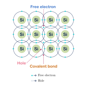
Let’s consider the Niels Bohr atomic model of the Silicon (Si) atom, Here I am considering only the valence shell of the Silicon (Si) atom and its covalent bond.
Here, whenever the valence electrons in the covalent bond get the required energy to break their bond, they will move as free electrons into the conduction band and leave their traces as holes in the valence band. How do the valence electrons get the required energy? The simple answer is, from the temperature. If we increase the temperature, there will be a lot of electron-hole pairs are generated in the semiconductors. After some time the conduction electrons are recombined with the holes by eliminating absorbed energy as either heat or light.
Atomic model and Energy band diagram for Silicon (Si) atom at a temperature (T) of 0 K :
At temperature T=0 K, the semiconductor acts like an insulator. This is seen from its atomic model at a temperature (T) of 0 K.
Atomic model at T = 0 K :
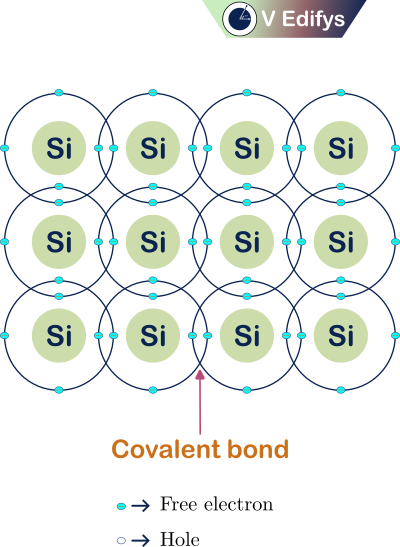
Here, I am representing the atomic model of the Intrinsic semiconductor Silicon (Si) atom. At T = 0 K, there are no free charge carriers in the semiconductor for electrical conduction, so it acts like an insulator. At the atomic level, the valence electrons in the Silicon atom didn’t get the required energy to break the covalent bond to free themself. So, there is no free (or) conduction electron in the semiconductor at T = 0 K.
Energy band diagram at T = 0 K :
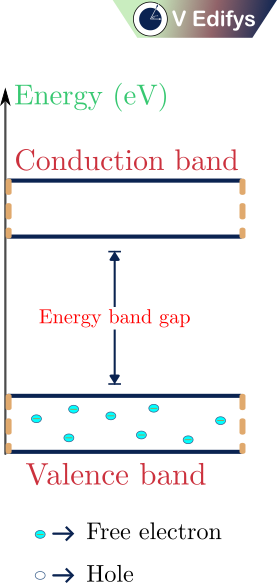
The above figure represents the energy band diagram of a semiconductor at a temperature of 0 K (T=0 K). The valence band is completely filled with electrons and conduction band is empty. Because, the electrons at a valence shell need energy to break the covalent bond to free themself as the free (or) conduction electrons. At T=0 K, the valence electrons didn’t get the needed energy to break the covalent bond, so all the valence electrons are placed in the valence band and there is no electrons in the conduction band. Likewise, no electrons move into the conduction band, so it doesn’t leave any traces in the valence band. As a result, there will be no holes in the valence band.
Atomic model and Energy band diagram for Silicon (Si) atom at room temperature (T = 300 K) :
At temperature T=300 K, the semiconductor starts to conduct some negligible value of electric current. This is seen from its atomic model at a temperature (T) of 300 K.
Atomic model at T = 300 K :
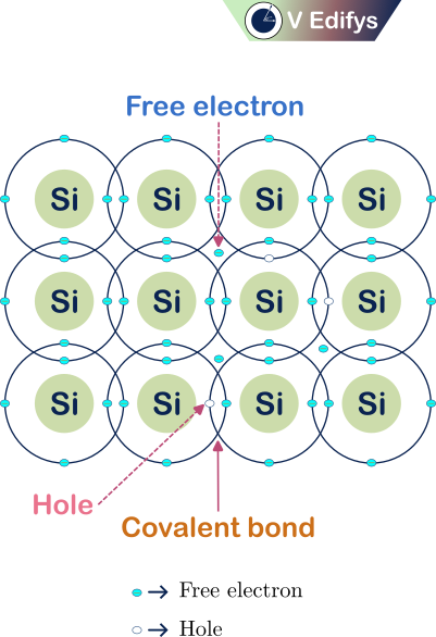
Here, I am representing the atomic model of the Intrinsic semiconductor Silicon (Si) atom. At T = 300 K, there are some free charge carriers are generated in the semiconductor for electrical conduction due to the increase in the temperature. At the atomic level, the valence electrons in the Silicon (Si) atom, get the required energy to break the covalent bond to free themself from the temperature. So, there are free (or) conduction electrons and the holes in the semiconductor at T = 300 K.
Energy band diagram at T = 300 K :
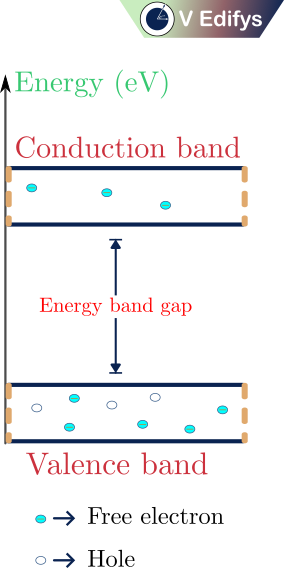
The above figure represents the energy band diagram of a semiconductor at a temperature of 300 K (T=300 K). At T=300 K, the valence electrons get the needed energy to break the covalent bond, so some of the valence electrons move into the conduction band and leave their traces as holes in the valence band. Due to the electrons in the conduction band and the holes in the valence band, electrical conduction is possible in the semiconductor at T=300 K. But the electrical conduction is very negligible, so we need another type of semiconductor called “Extrinsic semiconductor”.
The number of electrons moved into the conduction band is equal to the number of holes it is generated in the valence band. In other words, the total number of negative charges is equal to the total number of positive charges.
Equation of charge neutrality of semiconductors :
Even though we are performing doping operations to convert the intrinsic semiconductors to extrinsic semiconductors, the semiconductors will always be in a neutral state. How do I tell this? With the help of the law of electrical neutrality.
Law of electrical neutrality :
According to the law of electrical neutrality, the total number of positive charges in a material is equal to the total number of negative charges in the material.
i.e.,

where,
p = Hole concentration ( Unit : / cm3 )
n = Electron concentration ( Unit : / cm3 )
ND = Donor concentration ( Unit : / cm3 )
NA = Acceptor concentration ( Unit : / cm3 )
For Intrinsic semiconductors, the Donor concentration (ND) and the Acceptor concentration (NA) are equal to zero. Because in the intrinsic semiconductors, we are not doing doping operations.
What are Donor atoms and Acceptor atoms?
We all know that to increase the conductivity of a semiconductor we add some impurity atoms to the semiconductor atom, as a result, we get an extrinsic semiconductor. Depending on the impurity atom we get two types of extrinsic semiconductor, those are P-type semiconductor and N-type semiconductor.
- P-type : If we add a trivalent impurity atom to the Silicon (Si) atom, in the covalent bond between the Silicon and trivalent impurity atoms like ( Boron (B), Aluminium (Al), Gallium (Ga) etc., ) there will be a lack of one electron. That vacancy of the electron will be represented as a hole. The trivalent impurity atoms can be ready to accept one electron to fulfil their covalent bond with the Silicon atom. This is why the trivalent impurity atoms are called “Acceptor atoms” because they are ready to accept an electron.
- N-type : If we add a pentavalent impurity atom to the Silicon (Si) atom, in the covalent bond between the Silicon and pentavalent impurity atoms like ( Phosphorus (P), Arsenic (As), Antimony (Sb) etc., ) there will be an extra one electron. The pentavalent impurity atoms can be ready to give one excess electron to the semiconductor as a free electron. This is why the pentavalent impurity atoms are called “Donor atoms” because they are ready to give an electron.
Mass action law :
Mass action law states that the product of the electron concentration and the hole concentration is equal to the square of the intrinsic carrier concentration.
i.e.,
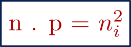
where,
n = Electron concentration ( Unit : / cm3 )
p = Hole concentration ( Unit : / cm3 )
ni = Intrinsic carrier concentration ( Unit : / cm3 )
Summary :
1. A particle which holds some sort of electric charge ( i.e. positive charge (or) negative charge ) is called a charge carrier.
2. Semiconductors are always be electrically neutral.
3. Mass action law
One Response
I’m extremely impressed along with your writing skills as smartly as with the layout on your weblog. Is this a paid topic or did you modify it yourself? Either way stay up the nice quality writing, it is uncommon to see a nice weblog like this one nowadays